2025-02-07 02:54:48|Myriagame |source:minecraft skins
According to an analysis of leaked Switch 2 motherboard photos, the Nintendo Switch 2's SoC may use Samsung's 5nm process instead of the 8nm process.
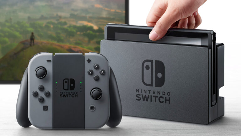
After yesterday's motherboard photos leaked, many users have been researching these components, trying to learn more about the console before the official announcement.According to an analysis published on Famiiboards, there is sufficient evidence that the Switch 2's SoC uses Samsung's 5nm process, rather than the 8nm process.
It is said that the Nvidia T239 chip that drives the Switch 2 has about 15 billion transistors. If the 8nm process is used, its area will reach 326mm^2, which is larger than the chip seen on the leaked motherboard.On the other hand, the area of the T239 chip is about 200mm^2, which is not only consistent with the Samsung 5nm process used for the Snapdragon 8 Gen1 chip, but also with the timeline, as the Snapdragon chip was released at the end of 2021, and the first batch of T239sThe project sample was released in April 2022.If this is true, then this definitely bodes well for the performance level of the system.
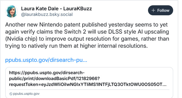
Another detail that has long been rumored but has not been officially confirmed is that Switch 2 supports Nvidia DLSS.Laura Kate Dale, a new Nintendo patent (filed earlier this week in the U.S.), strongly suggesting that the console will indeed use Nvidia-style AI scaling technology to improve output resolution.
In addition to amplifying lower input resolutions to 1080p and 4K resolutions, the main goal of the technology will be to keep the files smaller.

T2 believes that GTA6 violen
2025-02-12 23:28:04
The SIE State of Play launch
2025-02-12 23:28:00
"Midnight South" game durati
2025-02-12 23:27:57
"Pirate 4" sales exceeded 4
2025-02-12 23:27:54
"Assassin's Creed 3: Liberat
2025-02-12 23:27:50
"Assassin's Creed: Shadow" c
2025-02-12 23:27:47
Steam's new weekly sales lis
2025-02-12 23:27:44
"Hundred Days War Chronicle-
2025-02-12 23:27:41
Hideo Kojima will announce n
2025-02-12 23:27:38
"Civilization 7" Chinese are
2025-02-12 23:27:34
Pirate Minecraft Skins
Minecraft Skins
2024-12-10 04:11:27
Pirate Minecraft Skins
Minecraft Skins
2024-12-10 04:11:26
Master Minecraft Skins
Minecraft Skins
2024-12-10 04:11:25
King Minecraft Skins
Minecraft Skins
2024-12-10 04:11:25
Guide Minecraft Skins
Minecraft Skins
2024-12-10 04:11:24
Dark Knight Minecraft Skins
Minecraft Skins
2024-12-10 04:11:23
Sparta Minecraft Skins
Minecraft Skins
2024-12-10 04:11:23
Moncraft Skins of the War
Minecraft Skins
2024-12-10 04:11:22
Red Witch Minecraft Skins
Minecraft Skins
2024-12-10 04:11:22
Golden Cavaliers Minecraft S
Minecraft Skins
2024-12-10 04:11:22