2025-04-29 22:10:14|Myriagame |source:minecraft skins
The hardware core chip of Nintendo's new console Switch 2 seems to be confirmed.Promotion owner @Kurnalsalts posted a close-up photo of a part of the Switch 2 chipset that is said to be a Switch 2 chipset, confirming that the Switch 2 uses Nvidia's Tegra 239 chipset, which also calmed the debate on the Internet about the technical details of this hybrid host.
When the Switch 2 was released, we learned that it supports 4K/60FPS output (domain mode), but there is not much information about the core chip.It was previously known that Nintendo and Nvidia are partnering with custom Tegra SoCs, so it is speculated that the Switch 2 may use the next-generation Tegra 239 chip.
Now, this speculation has been confirmed. Netizen @Kurnalsalts shared a chip photo, which clearly marked "T239", which is Nvidia's Tegra 239 chip.
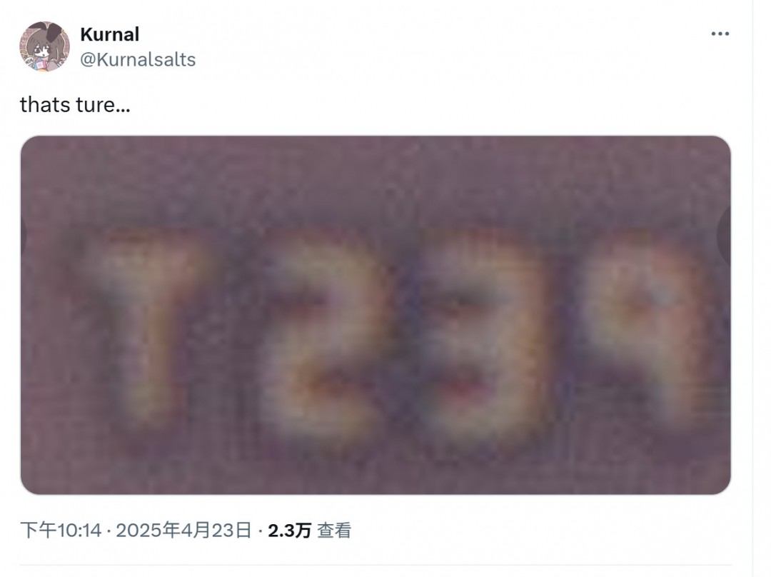
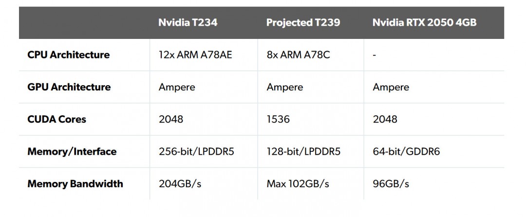
The photos did not provide more details, and the chip specifications still have to be speculated based on previous information.It is understood that the Tegra 239 is equipped with eight Arm Cortex-A78C cores, the GPU combines Ada Lovelace and Ampere architectures, and has 1,536 CUDA cores.The CPU main frequency is expected to be between 1.1 GHz and 1.5 GHz, depending on the base mode.In addition, it uses a 128-bit LPDDR5 memory interface.
According to a 2023 article published by Digital Foundry, here is a summary of key information about the NVIDIA T239 processor:
1. T239 Overview
Positioning: The T239 is the next generation Tegra processor customized by NVIDIA for Nintendo.
Origin: The T239 is based on NVIDIA's T234 processor (for the automotive and robotics sectors), but has been greatly cropped and optimized to suit the needs of mobile gaming devices.
Customization: Unlike the standard Tegra X1 used by the first Switch, the T239 is tailor-made for Nintendo consoles and includes specific game optimization features.
2. Technical specifications
CPU:
It adopts an octa-core ARM Cortex-A78C CPU cluster, suitable for gaming devices.
Unlike the T234's A78AE core, the A78C is more efficient, avoiding the core redundant verification design required in the automotive field.
GPU:
The Ampere architecture based on the NVIDIA RTX 30 series includes 1536 CUDA cores (about 75% of T234).
Some features are backported from the latest Ada Lovelace architecture (RTX 40 series), such as improved clock gating (improving low power efficiency) and media encoding/decoding modules (supporting formats such as AV1).
Supports hardware-accelerated ray tracing (RT) and DLSS upsampling, but without deep learning accelerator (DLA), DLSS processing relies entirely on the GPU's Tensor core.
Memory:
Equipped with a 128-bit LPDDR5 memory interface, it provides higher bandwidth, and solves the problem of memory bottlenecks of the first generation Switch.
It is speculated that the RAM capacity is 8-12GB, far exceeding the 4GB of the first generation Switch.
File Decompression Engine (FDE):
T239 has added a new hardware module, a PS5-like decompression block, which can quickly decompress the assets in storage into memory, significantly shortening the loading time (as rumored that Breath of the Wild" loading time is close to zero).
Other features:
NVIDIA supports NVN2 graphics API (an upgraded version of Switch graphics API), which is optimized for T239.
It contains optical flow accelerator (DLSS 3 frame generation core component), but because it is based on Ampere rather than Ada Lovelace, the frame generation effect may be limited.
3. Manufacturing process
8nm process: well-known leaker kopite7kimi says the T239 uses Samsung's 8nm DUV process (same as the RTX 30 series), but this raises concerns about power consumption and heat dissipation of handheld devices.
Process impact: Under the 8nm process, the T239 needs to operate at low frequency to control power consumption, similar to the low frequency strategy of the first generation Switch.
4. Performance
Simulation test: Digital Foundry uses RTX 2050 (Ampere architecture, 2048 CUDA core) to simulate T239 performance, and test games include "Cyberpunk 2077" and "Control" and so on:
At 720p resolution, the game can maintain 30fps, and the performance of 1080p is still smooth after DLSS is enabled, and it may reach 60fps after some optimizations.
4K DLSS upsampling is too expensive to compute for the T239 and may be difficult to achieve unless there is additional hardware support (such as the DLA of the T234).
Compare with PS4/Steam Deck:
The T239 performance is expected to outperform the PS4, but is lower than the PS4 Pro, close to or slightly better than the Steam Deck (7nm process, 163mm²).
Thanks to DLSS and modern architectures (ray tracing, grid shaders, etc.), the T239 can "overtake" its original performance in terms of image quality and efficiency.
limitation:
The 8nm process may limit performance and battery life and require low frequency operation to control power consumption.Ray tracing performance is limited, mobile GPU cycles are valuable, and RT may be used less in actual games.
Market positioning:
The T239 enables the Switch 2 to run optimized current-generation games (720p-1080p, some of which reach 1440p), but it cannot match the PS5/Xbox Series.
Combining DLSS and fast loading, the Switch 2 will provide a significantly better experience than the first generation of Switches, aiming to be a unique market that is portable and home-friendly.
5. Unsolved Mystery
Clock frequency: The exact frequency of T239 is unknown. The leaked information (January 2025) shows that the GPU is 1007MHz in dock mode, the CPU is 998.4MHz, and the memory bandwidth is 102.4GB/s, but further verification is required.
Process Confirmation: The dispute between 8nm and 5nm has not yet been concluded, and TechInsights and other institutions need to dismantle the final hardware confirmation.
DLSS efficiency: The T239's Tensor core is costly to run DLSS at low power consumption, and the actual effect requires more optimization and testing.
Summarize
The T239 is a customized Tegra chip created by NVIDIA for Nintendo Switch 2. It is based on the Ampere architecture (30 series graphics card), integrating some Ada Lovelace (40 series graphics card) features, and is equipped with an eight-core A78C CPU, 1536 CUDA core, LPDDR5 memory and file decompression engine.It supports ray tracing and DLSS, and its performance is expected to surpass PS4 and close to Steam Deck, and it can run optimized current-generation games (720p-1080p).The manufacturing process may be Samsung 8nm, affecting power consumption and performance.Although it is not a PS5-level hardware, the T239 significantly improves the Switch 2 experience through DLSS and fast loading, consolidating Nintendo's competitiveness in the hybrid console market.
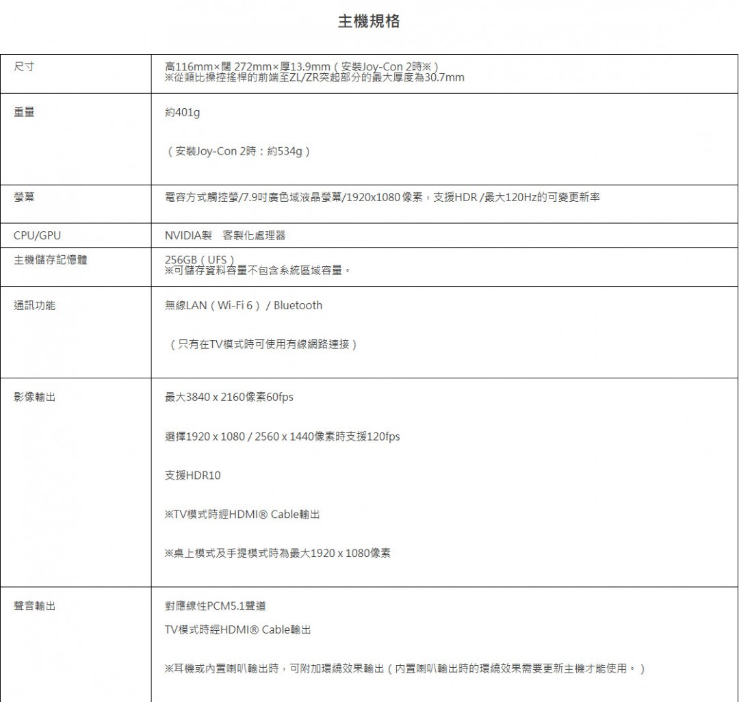
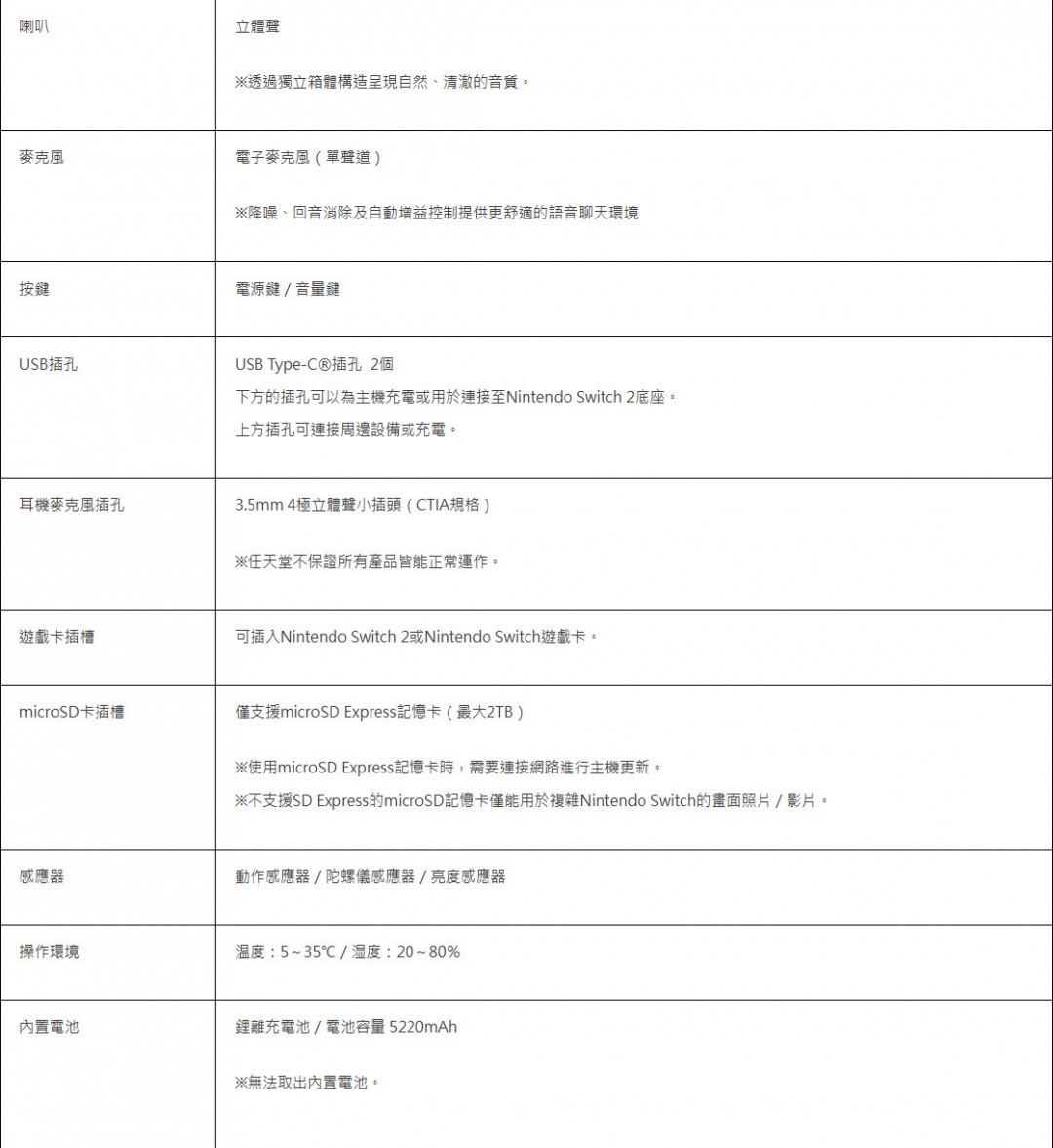
Previously, the Switch 2 specifications released by Nintendo's official website:

After the "Lost Lord" update
2025-04-29 22:16:51
"The Elder Scrolls 4: Annihi
2025-04-29 22:16:48
Former developer of "Starry
2025-04-29 22:16:45
High-energy warning!Comparis
2025-04-29 22:16:43
Fantasy card RPG "Knocking t
2025-04-29 22:16:40
"Shadow Blade Zero" is inspi
2025-04-29 22:16:37
After "Raiders of the Lost A
2025-04-29 22:16:32
The press conference of "The
2025-04-29 22:16:29
"Assassin's Creed" fans are
2025-04-29 22:16:26
Sony removes a number of mal
2025-04-29 22:16:24
Pirate Minecraft Skins
Minecraft Skins
2024-12-10 04:11:27
Pirate Minecraft Skins
Minecraft Skins
2024-12-10 04:11:26
King Minecraft Skins
Minecraft Skins
2024-12-10 04:11:25
Master Minecraft Skins
Minecraft Skins
2024-12-10 04:11:25
Guide Minecraft Skins
Minecraft Skins
2024-12-10 04:11:24
Sparta Minecraft Skins
Minecraft Skins
2024-12-10 04:11:23
Dark Knight Minecraft Skins
Minecraft Skins
2024-12-10 04:11:23
Golden Cavaliers Minecraft S
Minecraft Skins
2024-12-10 04:11:22
Red Witch Minecraft Skins
Minecraft Skins
2024-12-10 04:11:22
Moncraft Skins of the War
Minecraft Skins
2024-12-10 04:11:22